Semiconductor History | Ricoh Ikeda — Two Picture Processors Make Mode 7 Look Easy
volume_up
Listen
directions
Directions
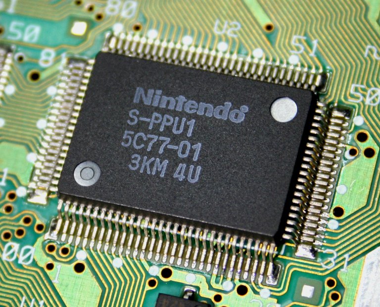
On 21 November 1990, Nintendo released the Super Famicom in Japan with a graphics system divided between two custom picture processors. Ricoh manufactured the 5C77, labelled S-PPU1, and the 5C78, labelled S-PPU2, as separate packages beside 64 kilobytes of video RAM.
The split let the chips spend their time on fixed display work rather than general computation. Together they fetched tilemaps and character data, evaluated sprites, combined layers by priority, applied palette and colour arithmetic, and produced the video signal while the 5A22 CPU ran the game.
The good was variety. Eight background modes traded colour depth, layer count, and resolution: one mode offered four low-colour backgrounds, the commonly used Mode 1 offered two 16-colour layers plus a four-colour layer, and other modes exchanged layers for 256-colour or high-resolution output.
A 256-entry colour memory selected from 32,768 possible colours. The PPUs could add or subtract the main and sub screens, clip them with windows, and mix sprites among background priorities, turning register settings into translucency, shadows, fog, and fades without drawing every pixel in software.
Mode 7 became the memorable demonstration. It applied an affine transform to one 128-by-128 tilemap, allowing that 1,024-by-1,024-pixel surface to rotate, scale, shear, or scroll; changing the transform by scanline through HDMA produced roads and landscapes that appeared to recede into depth.
The bad was that every mode was a bargain with the hardware. Mode 7 transformed one background rather than polygons, richer colour modes surrendered layers, and high-resolution modes narrowed other choices.
Programmers designed scenes around a table of mutually exclusive capabilities rather than a single unrestricted graphics pipeline.
Memory timing tightened the bargain. During normal display the PPUs owned video RAM, so the CPU could update it only during vertical blank or forced blank.
A game therefore had to schedule tile and map transfers into short intervals, often through DMA, while fitting the active graphics set into 64 kilobytes.
Sprites carried another visible limit: the system stored 128 objects, but only 32 sprites and 34 eight-pixel slivers could survive evaluation on one scanline. Crowded scenes could make lower-priority pieces disappear, turning character placement into bandwidth management.
This architecture explains both the Super Famicom’s visual identity and its programming reputation. The two PPUs made elaborate tiled scenes economical, yet the best results came from artists and engineers who understood exactly which layer, palette, scanline, and blanking interval they could spend.
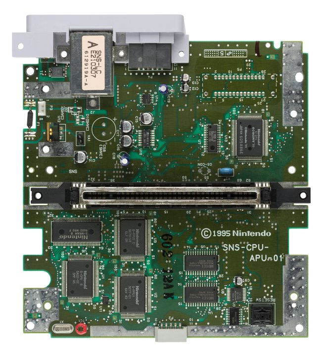
The cover shows a later S-PPU1 5C77-01, not a launch-revision chip. The second photograph shows both PPUs on a 1995 SNS-CPU-APU-01 three-chip motherboard, providing system context rather than a picture of the 1990 production line.
The pin marks today’s Nisshinbo Micro Devices Ikeda Office, successor to Ricoh’s semiconductor operations. It is an institutional lineage marker, not a claim that the present building was the exact PPU design room or fabrication line.
Sources:
Nintendo, Super Nintendo Entertainment System Development Manual, Book I: https://floating.muncher.se/bot/manual/book1_text.pdf
Nintendo, “Iwata Asks: Star Fox 64 3D”: https://www.nintendo.com/en-za/Iwata-Asks/Iwata-Asks-Star-Fox-64/Vol-1-Star-Fox-64-3D/2-It-ll-Be-Easy-to-Make-/2-It-ll-Be-Easy-to-Make--220848.html
SNESdev Wiki, “Backgrounds”: https://snes.nesdev.org/wiki/Backgrounds
SNESdev Wiki, “Reading and writing PPU memory”: https://snes.nesdev.org/wiki/Reading_and_writing_PPU_memory
SNESdev Wiki, “Sprites”: https://snes.nesdev.org/wiki/Sprites
Fabien Sanglard, “How the SNES Graphics System Works”: https://fabiensanglard.net/snes_ppus_how/
Photos:
Yaca2671, “5C77-01 01.jpg,” CC BY-SA 3.0: https://commons.wikimedia.org/wiki/File:5C77-01_01.jpg
Evan-Amos, “Nintendo-Super-NES-Mk1-Motherboard-Top.jpg,” public domain: https://commons.wikimedia.org/wiki/File:Nintendo-Super-NES-Mk1-Motherboard-Top.jpg



















































































































 expand_more