Semiconductor History | SCREEN Kyoto — Printing Chemistry Becomes Wafer Equipment
volume_up
Listen
directions
Directions
In November 1975, Dainippon Screen Manufacturing—now SCREEN Holdings—began producing and selling its EMW-322 and EMW-411 wafer-etching systems. The move took a Kyoto company rooted in photographic and printing equipment into the machinery used to shape semiconductor wafers.
The transition was less surprising than it first appears. Printing and chipmaking both depend on coating a surface, exposing a pattern, developing it, removing selected material, and cleaning what remains. SCREEN could recombine knowledge of photosensitive chemistry, fluid handling, precision motion, and surface treatment rather than invent an equipment culture from nothing.
The good result was a durable specialty. SCREEN followed the etchers with spinner equipment in 1978 and built a major position in wafer cleaning, where microscopic particles or chemical residue can destroy devices. The company’s history shows how expertise from an older image industry could migrate into the semiconductor supply chain and remain useful across many generations of chips.
The bad side is that equipment success inherits the chip industry’s volatility. A toolmaker must fund engineering, demonstration systems, service, and factory capacity before a customer’s capital budget becomes certain. When memory or logic producers delay new fabs, an equipment supplier can experience an abrupt order contraction even if its technology remains competitive.
Cleaning and etching also carry environmental costs. They consume ultrapure water and tightly controlled chemicals, create liquid and gaseous waste streams, and require facilities that protect both workers and wafers. Better tools reduce contamination and chemical use per successful wafer, but rising wafer volumes and more process steps can offset those gains.
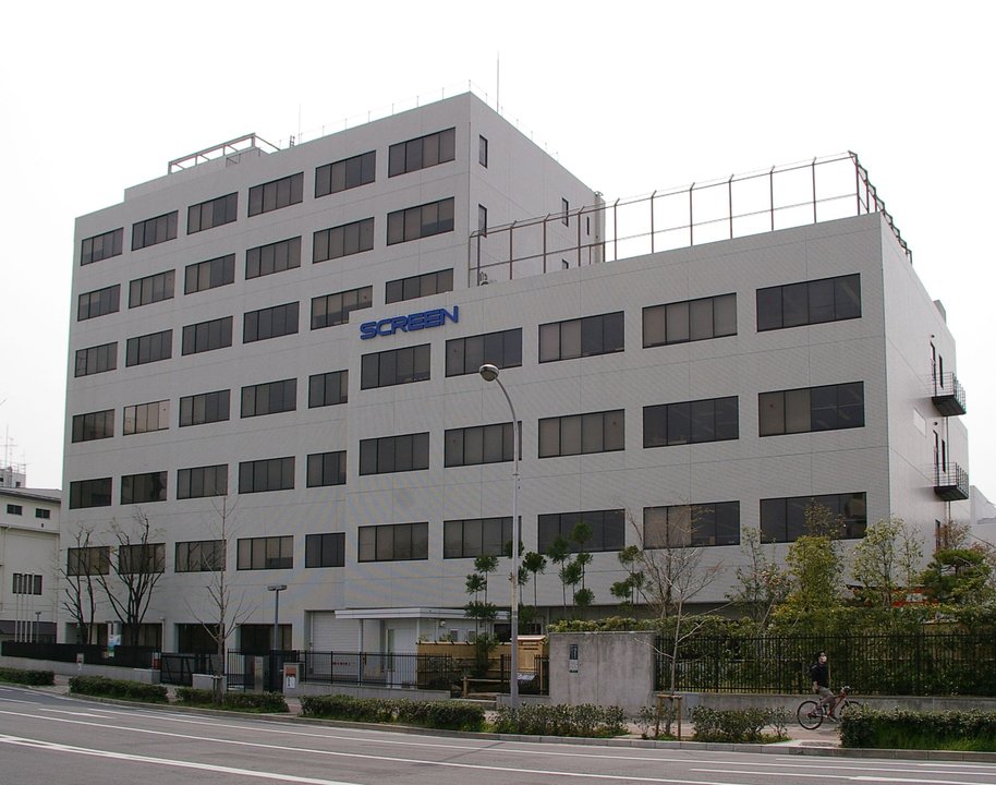
SCREEN’s semiconductor operations were strengthened at its Hikone facilities, so the pictured Kyoto headquarters should not be mistaken for the original 1975 manufacturing line. It is the verified public corporate anchor for the decision and the continuing company; the site distinction is part of the memory rather than hidden by the pin.
Sources: [SCREEN corporate history, 1968–1979](https://www.screen.co.jp/en/about/history_3); [SCREEN corporate history, 2000–2009](https://www.screen.co.jp/en/about/history_4); [SCREEN 2018 offering circular hosted by SGX](https://links.sgx.com/FileOpen/SCREEN%20Holdings%20CB%202018.ashx?App=Prospectus&FileID=35091); [The Shashi company history of SCREEN](https://the-shashi.com/tse/7735/).
Photo: J o, CC BY-SA 3.0, via Wikimedia Commons.
## 3. Semiconductor History|TOK Nakamaruko — The Light-Sensitive Film Between Mask and Silicon



















































































































 expand_more