

- Home
- Semiconductor History | Japan | From Nihonbashi to Chitose
- Semiconductor History | HOYA Nakaochiai — Optical Glass Becomes the Mask's Foundation
Semiconductor History | HOYA Nakaochiai — Optical Glass Becomes the Mask's Foundation
· 1974-1
Personal memoryBy kevin · · Report an issue

Find memories left by people near you.
Distribute Bounty
This will distribute the bounty equally among all qualifying memories. This action cannot be undone.
Cancel Bounty
Are you sure you want to cancel this bounty? The remaining amount will be refunded to your account.
Success!
Operation completed successfully.
Error
Something went wrong.
Semiconductor History | HOYA Nakaochiai — Optical Glass Becomes the Mask's Foundation
kevin

In January 1974, HOYA began producing glass substrates for integrated-circuit masks. The work took a company founded to make optical glass into the semiconductor lithography supply chain, where a nearly perfect glass plate becomes the foundation for the pattern used to print circuits onto wafers.
A mask blank looks simple, but its surface must be extremely flat, smooth, clean, and free of defects before an opaque film and circuit pattern are added. HOYA could transfer skills in glass melting, polishing, optical inspection, and contamination control from lenses and other precision products into this demanding intermediate material.


The good outcome was specialization at a critical bottleneck. A mask blank does not compute anything, yet poor glass can ruin the master pattern used across many wafers. As circuit dimensions shrank, accumulated control of materials and surfaces became more valuable. HOYA's position also showed that Japan's semiconductor strength extended beyond famous chip brands into enabling materials.


The bad side is disproportionate liability. One hidden defect can waste costly mask writing, inspection, and fab time, so qualification is lengthy and customers are conservative about changing suppliers. The producer must invest ahead of demand in cleaner facilities and finer measurement while selling into a market tied to the uneven timing of customers' new process nodes.
Mask blanks are not ordinary consumables replaced after every wafer. Their demand can therefore swing with design activity and technology transitions rather than wafer volume alone. A small number of advanced customers also gain bargaining power, and geopolitical controls can turn an optical-material business into strategic infrastructure.
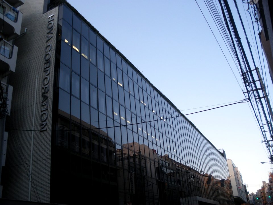
Production began at HOYA's Nagasaka plant in Yamanashi, not at Nakaochiai. The pictured headquarters was completed later, in 1984, and HOYA moved its group headquarters to Nishi-Shinjuku in 2016; the former site now has another use. The pin intentionally marks the photographed corporate building associated with the company, while the narrative preserves the true manufacturing location.
Sources: [HOYA corporate history](https://www.hoya.com/en/company/history/); [SEMI Innovation Stories account of the 1974 mask-blank launch](https://www.semi.org/sites/semi.org/files/docs/Innovation%20Stories%201_Web.pdf); [HOYA information-technology business review](https://www.hoya.com/ir/2022/en/review/it.html); [HOYA mask-blank technology overview](https://www.hoya.com/en/business/it/).
Photo: Kentin, CC BY-SA 3.0, via Wikimedia Commons.
changes?
delete this memory?
We detected that you have a Blox in your crypto wallet! We will import the Blox into your account.
Click on done below to complete the import.
Welcome Back!
Sign in to preserve cherished moments
Don't have an account?
Welcome!!
Sign up and start preserving cherished moments
?
?

Choose your payment method
Buy with Metablox Credit
Do you want to mint Blox with Metablox Credit?
Which Crypto would you like to use?
Purchase Confirmed!
Your Blox is being minted on-chain and will appear in your profile shortly.
Log in or sign up to claim your Blox.
How many credits do you want to buy?
$100 USD = 1 Metablox Credit = 1 Blox.
Use Metablox Credit to mint any Blox you want on the map.
expand_more








































































































