

- Home
- Semiconductor History | Japan | From Nihonbashi to Chitose
- Semiconductor History | MARUWA Owariasahi — Pottery Becomes a Heat Path
Semiconductor History | MARUWA Owariasahi — Pottery Becomes a Heat Path
· 1973-4
Personal memoryBy kevin · · updated · Report an issue

Find memories left by people near you.
Distribute Bounty
This will distribute the bounty equally among all qualifying memories. This action cannot be undone.
Cancel Bounty
Are you sure you want to cancel this bounty? The remaining amount will be refunded to your account.
Success!
Operation completed successfully.
Error
Something went wrong.
Semiconductor History | MARUWA Owariasahi — Pottery Becomes a Heat Path
kevin

MARUWA Ceramic Co., Ltd. was established on April 5, 1973, after a family ceramics lineage that the company traces to the early nineteenth century. In 1974 it began producing ceramic substrates for chip resistors, formalizing a shift already under way in the 1960s from tableware toward specialty ceramics for communications and electronic components.

A ceramic substrate is both floor and heat path. Conductive patterns and components can be built on an electrically insulating plate that tolerates heat, chemicals, and dimensional stress better than many organic materials. MARUWA later expanded from alumina into aluminum nitride, silicon nitride, metallized and multilayer substrates, ultra-high-purity silicon-carbide parts, and quartz products used in semiconductor equipment.


The good was continuity without stagnation. Skills in powder preparation, forming, firing, and controlling shrinkage could be redirected from porcelain into components with tightly specified electrical and thermal behavior. Modern power semiconductors and manufacturing tools need materials that move heat, resist plasma and corrosion, or remain clean at high temperature; ceramics give Japan a valuable position around the chip even when the silicon die is fabricated elsewhere.

The bad is that advanced ceramics remain unforgiving physical products. Firing consumes substantial energy, dimensional defects may appear only after long processing, and brittle parts can crack during machining, assembly, or thermal cycling. High-purity feedstock and clean finishing add cost. Qualification creates customer trust but also long sales cycles, and capacity must be expanded carefully because semiconductor demand can reverse before a new kiln or machining line pays back.
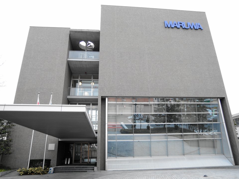
The pin and cover identify MARUWA’s current Owariasahi headquarters, to which the company moved in 1997, not the original 1973 office or a public factory tour. The building is used as the corporate anchor for a lineage that began in Seto-region ceramics and grew into semiconductor materials.
Sources: MARUWA corporate profile and history; MARUWA semiconductor-equipment product directory; MARUWA business overview and quartz-glass product pages.
Photo: “Headquarters of MARUWA,” アラツク, CC BY-SA 4.0. https://commons.wikimedia.org/wiki/File:Headquarters_of_MARUWA.JPG
changes?
delete this memory?
We detected that you have a Blox in your crypto wallet! We will import the Blox into your account.
Click on done below to complete the import.
Welcome Back!
Sign in to preserve cherished moments
Don't have an account?
Welcome!!
Sign up and start preserving cherished moments
?
?

Choose your payment method
Buy with Metablox Credit
Do you want to mint Blox with Metablox Credit?
Which Crypto would you like to use?
Purchase Confirmed!
Your Blox is being minted on-chain and will appear in your profile shortly.
Log in or sign up to claim your Blox.
How many credits do you want to buy?
$100 USD = 1 Metablox Credit = 1 Blox.
Use Metablox Credit to mint any Blox you want on the map.
expand_more








































































































