Semiconductor History | ROHM Chikugo — Silicon Carbide Leaves the Laboratory
volume_up
Listen
directions
Directions
On December 21, 2010, ROHM announced that it had developed and begun mass production of a silicon-carbide double-diffused MOSFET. Its company history records the December milestone as the first mass production of a SiC DMOSFET, moving a promising laboratory material into repeatable industrial output.
The front-end work was assigned to ROHM Apollo Device in Fukuoka Prefecture. ROHM’s Chikugo plant at 883 Kamikitajima is the group’s SiC-device wafer-processing site, and later capacity expansions there made the geography of that 2010 bet unmistakable.
The good was efficiency under punishment. Silicon carbide can block high voltages while switching faster and losing less energy than conventional silicon power devices, attributes that became especially valuable in electric-vehicle inverters and onboard chargers.
Less loss means less waste heat, potentially smaller cooling hardware, and more battery energy reaching the road.
ROHM also attacked the manufacturing problem as a chain rather than a single chip. The 2010 announcement named SiCrystal in Germany for wafers, Fukuoka for front-end device fabrication, and ROHM Integrated Systems in Thailand for back-end work.
After acquiring SiCrystal in 2009, ROHM could connect substrate, device design, wafer processing, packaging, and screening inside one group.
The bad was embedded in the press release itself. Crystal defects threatened reliability, while the high-temperature process produced variations in device characteristics.
ROHM said proprietary process technology and screening overcame those obstacles, but screening is also an admission that wide-bandgap performance arrives with yield, consistency, and qualification costs.
Automotive use raised the bar further. A transistor that looks excellent on a bench must survive years of heat cycles, vibration, voltage spikes, and safety scrutiny, and a vertically integrated chain still crosses national borders and multiple factories.
Better material physics did not abolish manufacturing risk; it moved the industry into a harder manufacturing regime.
Chikugo later became a visible scale-up site. ROHM completed a five-story SiC production building there in December 2020 and began installing equipment in 2021, pairing growth with seismic isolation, flood countermeasures, emergency generation, and renewable electricity.
The expansion shows both sides of the story: SiC had become strategically valuable, and making enough reliable devices required far more than the 2010 breakthrough.
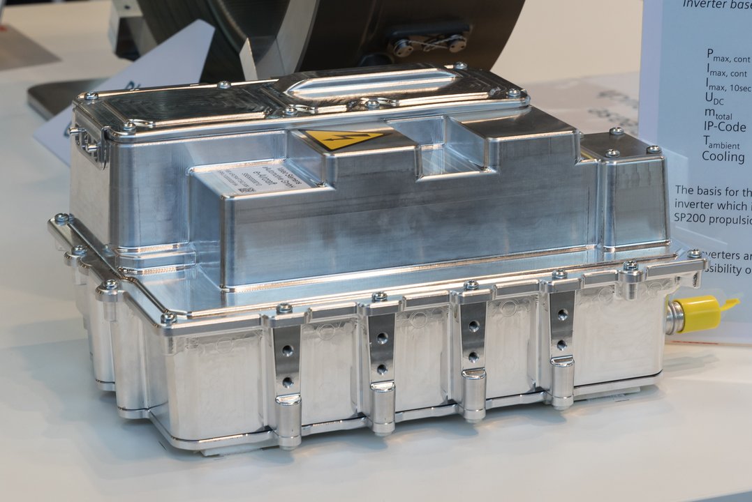
The cover shows a Valeo SiC MOSFET inverter displayed at AERO Friedrichshafen in 2018. It is not a ROHM product or a photograph of the Chikugo line; it depicts the power-conversion system that this class of device ultimately serves.
Sources: ROHM, “The World’s First Low On-Resistance High-Speed SiC Transistor (DMOSFET),” 21 December 2010; ROHM company history; ROHM Chikugo plant location profile; ROHM, “Completes Construction of a New Environmentally Friendly Building at its Apollo Chikugo,” 18 January 2021; Mapion exact-address listing.
Photo: Matti Blume, CC BY-SA 4.0, via Wikimedia Commons.



















































































































 expand_more