Semiconductor History | Nintendo Fukuine — DMG-CPU Puts the Game Boy’s Core on One Chip
volume_up
Listen
directions
Directions
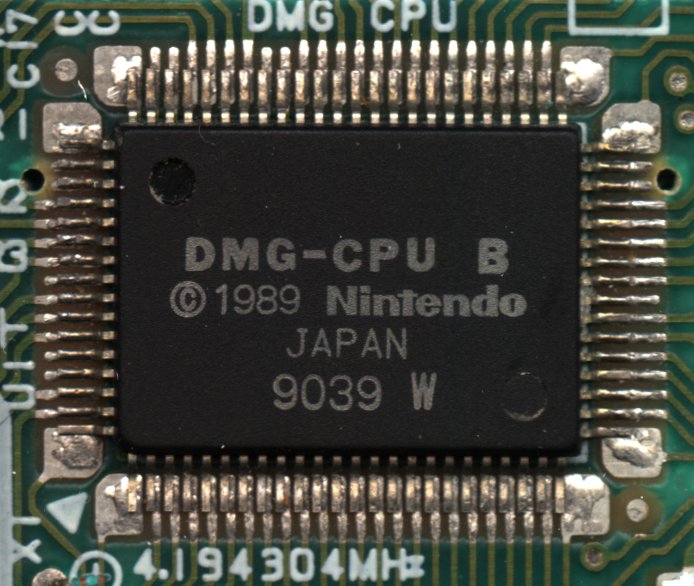
On 21 April 1989, Nintendo released the Game Boy in Japan with its central circuitry gathered into one large square package marked DMG-CPU. That custom system-on-chip gave a modest handheld one stable electronic heart.
The Nintendo-marked, Sharp-manufactured chip combined an SM83-compatible eight-bit CPU core with the picture-processing unit, four-channel audio, DMA, timers, serial link, interrupt control, and other system logic. Its 4.194304-megahertz master clock coordinated a machine designed around a 160-by-144-pixel display and four visible shades.
The good was concentration and consistency. Instead of assembling a handheld from many general-purpose chips, Nintendo and Sharp gave every ordinary Game Boy the same tightly defined platform, while cartridges supplied program and game data.
That platform was simple enough to learn deeply. Tile-based graphics, hardware sprites, fixed audio channels, and a serial port became dependable tools; programmers could optimize against the same timing rules for years, and the link hardware made direct two-player communication part of the console rather than an aftermarket invention.
DMA illustrates the economy. A transfer could copy 160 bytes of sprite-attribute data into OAM without making the CPU move each byte itself, leaving the processor to organize game logic around the display's rigid schedule.
The bad was scarcity. The system exposed only 8 KiB of work RAM and 8 KiB of video RAM, the monochrome screen could show four shades, and only ten sprites could appear on one scanline even though forty could be defined for the whole screen.
The picture processor also owned video memory during parts of each scanline. CPU reads or writes to VRAM and sprite memory could be blocked while the PPU was using them, so smooth animation depended on scheduling updates during narrow safe periods.
Its CPU is often casually called a Z80 or “LR35902,” but neither label is an official description of the complete chip. The instruction set resembles the Intel 8080 and Zilog Z80 families while removing or changing important features, so code written for either processor could not simply run unchanged.
Those limits were not incidental: they shaped Game Boy art, flicker, sound drivers, and engine design. The same restrictions that made the hardware economical also forced developers to treat memory, sprites, and every display interval as scarce resources.
The cover photograph shows a later DMG-CPU B package, not the launch-revision DMG-CPU. Its markings include ©1989 Nintendo, JAPAN, and DMG-CPU B, while the nearby board crystal is marked 4.194304 MHz.
The pin marks Nintendo's documented headquarters at 60 Fukuine Kamitakamatsu-cho when Game Boy launched. The surviving former headquarters, now Nintendo's Kyoto Research Center, is a corporate and development anchor—not a claim that Sharp fabricated the chip there or that its exact design desk is known.
Sources:
Nintendo, “Game Boy Series Sales Top 100 Million,” 11 March 2009: https://www.nintendo.co.jp/corporate/release/2009/090311.html
Nintendo, original Game Boy hardware archive: https://www.nintendo.co.jp/n02/dmg/hardware/gb/index.html
Nintendo, corporate history: https://www.nintendo.co.jp/corporate/en/history/index.html
Gekkio, Game Boy: Complete Technical Reference: https://gekkio.fi/files/gb-docs/gbctr.pdf
Pan Docs, specifications, rendering, memory map, audio, and CPU comparison: https://gbdev.io/pandocs/
Asahi Shimbun, Game Boy retrospective: https://smbiz.asahi.com/article/14605034
Photo:
ZyMOS, “Ic-photo-Nintendo--DMG-CPU B--(Gameboy-CPU).png,” CC BY-SA 4.0, via Wikimedia Commons: https://commons.wikimedia.org/wiki/File:Ic-photo-Nintendo--DMG-CPU_B--(Gameboy-CPU).png



















































































































 expand_more