

- Home
- Semiconductor History | Japan | From Nihonbashi to Chitose
- Semiconductor History | Mitsui High-tec Komine — Stamping the Frame Around the Chip
Semiconductor History | Mitsui High-tec Komine — Stamping the Frame Around the Chip
· 1969-6
Personal memoryBy kevin · · updated · Report an issue

Find memories left by people near you.
Distribute Bounty
This will distribute the bounty equally among all qualifying memories. This action cannot be undone.
Cancel Bounty
Are you sure you want to cancel this bounty? The remaining amount will be refunded to your account.
Success!
Operation completed successfully.
Error
Something went wrong.
Semiconductor History | Mitsui High-tec Komine — Stamping the Frame Around the Chip
kevin

In June 1969, Mitsui High-tec began mass production and sale of stamped IC leadframes using tungsten-carbide progressive dies. A national industrial-technology record dates the preserved die to 1969 and credits the approach with cutting the cost of the older photo-etching route to roughly one tenth.
A leadframe is the metal skeleton around many packaged chips. Its inner leads connect to the die by tiny wires, its outer leads connect the package to a circuit board, and its shape must remain consistent through plating, bonding, molding, trimming, and forming.

The good side of stamping was speed. A progressive die performs several operations as a metal strip advances through the press, allowing large numbers of nearly identical frames to emerge from a process built for repetition.
Tungsten carbide mattered because the features were small and the production runs long. The tool had to resist wear while holding tight dimensions; a die company that could grind and maintain such tooling could turn packaging hardware from a costly specialty into a mass-produced component.



That change helped semiconductor assembly scale. Cheap, repeatable leadframes supported the spread of plastic IC packages through calculators, appliances, automobiles, and industrial controls, even though the metal frame remained largely invisible beneath black molding compound.
The bad side sits in the mechanics. Stamping can create burrs, residual stress, dimensional drift, and tool wear, and every improvement in lead pitch makes die alignment and maintenance harder; one damaged station can repeat the same defect across a large lot.
The success also created exposure. Leadframes became price-sensitive, assembly moved across borders, package formats changed, and later products such as ball-grid arrays and advanced substrates reduced the frame’s role in parts of the market.
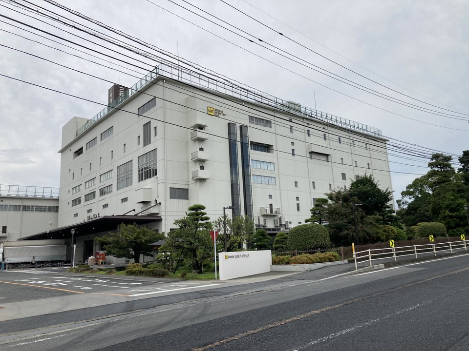
Komine is more than a symbolic headquarters pin: Mitsui built its Komine plant here in 1960, before the leadframe breakthrough. The current building is later, but the site preserves the geographic continuity between the company’s toolmaking roots and its semiconductor business.
Sources: [Mitsui High-tec company history](https://mitsui-high-tec.eu/company-history/); [National Museum of Nature and Science record for the 1969 die](https://sts.kahaku.go.jp/sts/detail.php?c=&city=&id=&no=116012130002&org=&p=1185&pref=&word=&y1=&y2=); [Mitsui High-tec Japanese history](https://www.mitsui-high-tec.com/about/history/); [official headquarters profile](https://www.mitsui-high-tec.com/company/about/).
Photo: RGloucester, CC0 1.0, via Wikimedia Commons.
changes?
delete this memory?
We detected that you have a Blox in your crypto wallet! We will import the Blox into your account.
Click on done below to complete the import.
Welcome Back!
Sign in to preserve cherished moments
Don't have an account?
Welcome!!
Sign up and start preserving cherished moments
?
?

Choose your payment method
Buy with Metablox Credit
Do you want to mint Blox with Metablox Credit?
Which Crypto would you like to use?
Purchase Confirmed!
Your Blox is being minted on-chain and will appear in your profile shortly.
Log in or sign up to claim your Blox.
How many credits do you want to buy?
$100 USD = 1 Metablox Credit = 1 Blox.
Use Metablox Credit to mint any Blox you want on the map.
expand_more








































































































