Semiconductor History | JEOL Akishima — Electron Optics Draws the Mask, One Beam at a Time
volume_up
Listen
directions
Directions
In 1998, JEOL completed the JBX-9000MV electron-beam lithography system. A contemporary JEOL technical history describes it as a machine developed to write the masks for 256-megabit DRAMs and later devices—an application where electron optics could define patterns finer than an ordinary optical writer.
The step was a natural extension of an unusual corporate lineage. JEOL had built electron microscopes, completed its JSM-1 scanning electron microscope in 1966, and entered electron-beam metrology and focused-ion-beam equipment in the 1980s. The same disciplines—electron sources, lenses, deflection, vacuum, vibration control, and precise stages—could be recombined to manufacture the master patterns used by chip lithography.
The good side is resolution and flexibility. An electron beam can directly write complex features into a resist without first projecting them through another mask. That makes electron-beam lithography indispensable for photomask fabrication and valuable for research, prototyping, and nanostructures where pattern freedom matters more than wafer-per-hour output.
The bad side is contained in the phrase “write.” A conventional beam traces a design serially, pixel by pixel, while optical exposure transfers a large field in parallel. Academic reviews identify throughput as electron-beam lithography’s central manufacturing limitation; charging, electron scattering, drift, and proximity effects add further process-control burdens.
JEOL’s accomplishment therefore did not displace optical lithography on production wafers. It occupied a narrower but essential layer of the ecosystem: making and measuring the masks that optical scanners reproduce many times. This is a recurring feature of semiconductor history—an apparently slower technology can remain strategically important because it creates the tool used by the faster one.
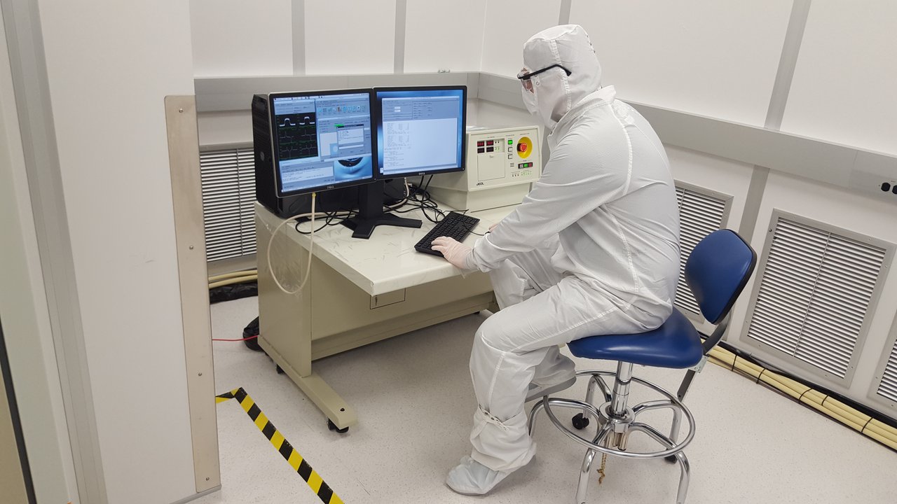
The photograph shows a later JEOL electron-beam lithography system in use at Simon Fraser University in Canada. It is an artifact image, not the 1998 JBX-9000MV and not a scene inside JEOL’s Akishima headquarters; the pin marks the Japanese company base from which the equipment lineage was managed.
Sources: [JEOL corporate milestones](https://www.jeol.com/corporate/outline/history.php); [JEOL News, July 1999](https://www.jeolusa.com/Portals/2/jeolnews/JEOL%20News%20July%201999%20Vol.%2034%20No.%201.pdf?ver=1dUKHE1oU6ibwmDNmzoWWQ%3D%3D); [Microelectronic Engineering review of electron-beam throughput](https://doi.org/10.1016/S0167-9317(02)00528-2); [EPFL electron-beam lithography description](https://www.epfl.ch/research/facilities/cmi/equipment/ebeam-lithography/raith-ebpg5000/tool-description/).
Photo: Simon Fraser University - Communications & Marketing, CC BY 2.0, via Wikimedia Commons.



















































































































 expand_more