

- Home
- Semiconductor History | Japan | From Nihonbashi to Chitose
- Semiconductor History | Yokkaichi Fab — From DRAM Retreat to NAND Scale
Semiconductor History | Yokkaichi Fab — From DRAM Retreat to NAND Scale
· 1992
Personal memoryBy kevin · · updated · Report an issue

Find memories left by people near you.
Distribute Bounty
This will distribute the bounty equally among all qualifying memories. This action cannot be undone.
Cancel Bounty
Are you sure you want to cancel this bounty? The remaining amount will be refunded to your account.
Success!
Operation completed successfully.
Error
Something went wrong.
Semiconductor History | Yokkaichi Fab — From DRAM Retreat to NAND Scale
kevin

Toshiba established its Yokkaichi semiconductor plant in 1992 to manufacture 16-megabit DRAM. It was a late high-volume move into a market already defined by steep price cycles, but the site’s more consequential history began when NAND flash production started there in 1999.



The change of product was the good decision. As Japanese firms retreated from commodity DRAM, Yokkaichi became a long-lived manufacturing base for flash, accumulating the process knowledge, clean-room infrastructure, and production scale needed to keep a Japanese company near the front of nonvolatile memory.

Scale brought its own risks. Each generation demanded heavier capital spending, closer coordination with equipment and materials suppliers, and high utilization across enormous facilities, so a technically successful fab remained exposed to price collapses, demand shocks, and the financing problems of its parent.
Ownership changed around the factory even while wafers continued moving through it. Toshiba separated the memory business as Toshiba Memory in 2017, and the company adopted the Kioxia name in 2019, making Yokkaichi both a symbol of continuity and evidence of how corporate survival can require a break with the old identity.
This is why Yokkaichi belongs in both the good and bad columns of Japan’s semiconductor history. It demonstrates adaptation after the DRAM era and preserves deep manufacturing capability, but it also shows the narrow path left to an integrated memory producer when fabrication leadership requires recurring investments measured on a global scale.
The site did not single-handedly reverse Japan’s broader decline in logic chips, personal-computer platforms, or fabless design. What it did was more specific and durable: it carried one major Japanese invention into mass production through successive corporate and technological transitions.
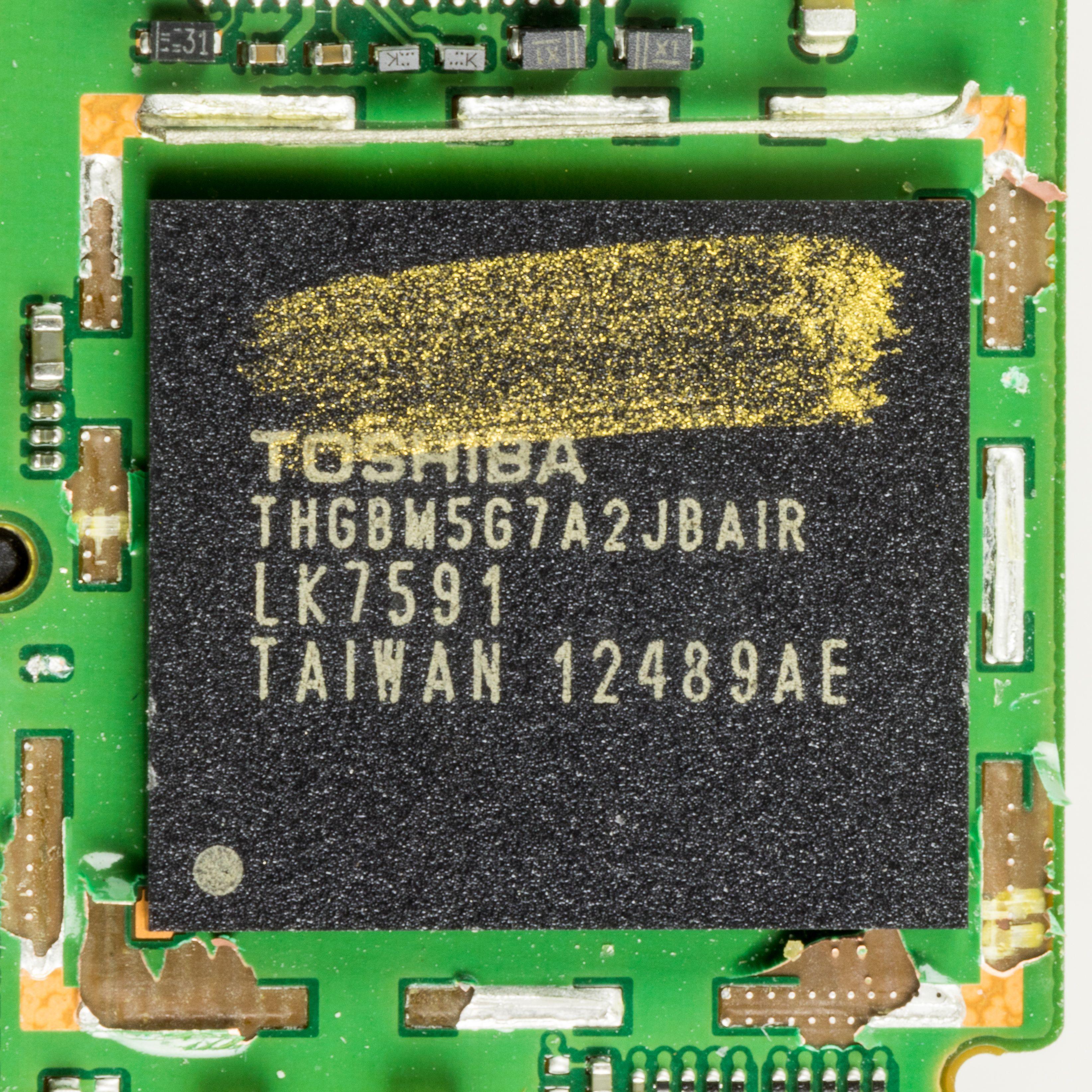
The photograph shows a later Toshiba-branded NAND package mounted inside an LG Nexus 4, not the Yokkaichi buildings; the pin marks the manufacturing site where Toshiba began NAND production in 1999. Image by Raimond Spekking, licensed CC BY-SA 4.0 via Wikimedia Commons.
changes?
delete this memory?
We detected that you have a Blox in your crypto wallet! We will import the Blox into your account.
Click on done below to complete the import.
Welcome Back!
Sign in to preserve cherished moments
Don't have an account?
Welcome!!
Sign up and start preserving cherished moments
?
?

Choose your payment method
Buy with Metablox Credit
Do you want to mint Blox with Metablox Credit?
Which Crypto would you like to use?
Purchase Confirmed!
Your Blox is being minted on-chain and will appear in your profile shortly.
Log in or sign up to claim your Blox.
How many credits do you want to buy?
$100 USD = 1 Metablox Credit = 1 Blox.
Use Metablox Credit to mint any Blox you want on the map.
expand_more








































































































