

- Home
- Semiconductor History | Japan | From Nihonbashi to Chitose
- Semiconductor History | Hitachi Naka — The Microscope Becomes a Yield Tool
Semiconductor History | Hitachi Naka — The Microscope Becomes a Yield Tool
· 1984
Personal memoryBy kevin · · Report an issue

Find memories left by people near you.
Distribute Bounty
This will distribute the bounty equally among all qualifying memories. This action cannot be undone.
Cancel Bounty
Are you sure you want to cancel this bounty? The remaining amount will be refunded to your account.
Success!
Operation completed successfully.
Error
Something went wrong.
Semiconductor History | Hitachi Naka — The Microscope Becomes a Yield Tool
kevin

In 1984, Hitachi’s Naka Works launched the S-6000, described by the company as the world’s first critical-dimension scanning electron microscope for semiconductor devices. Conventional optical inspection was approaching its limit as VLSI circuit lines moved below one micrometer. Hitachi turned the electron microscope from an instrument that showed structures into a production tool that measured them.
A CD-SEM scans a focused electron beam across a patterned wafer and calculates the width and shape of features. That measurement closes the loop between lithography, etching, and process control: engineers can see whether a line is drifting before the error becomes thousands of bad chips. The first S-6000 went to a Hitachi device-development center, followed by production use at the Musashi Works.
The good was yield through feedback. Naka combined electron optics, vacuum systems, detectors, stages, image processing, and factory automation into a tool fabs could trust repeatedly. The product created a durable Japanese position in semiconductor metrology, and later generations measured ever-smaller patterns while defect-review systems expanded the role of electron beams on production floors.


The bad is that measurement itself can become a bottleneck. Electron-beam inspection is slower than broad optical methods, insulating samples can charge, and excessive exposure may alter sensitive resist. Tools are expensive, complicated, and dependent on precision components and expert service. Fabs must decide where to sample rather than inspect everything, while the supplier’s revenue remains tied to concentrated customers and volatile capital-spending cycles.
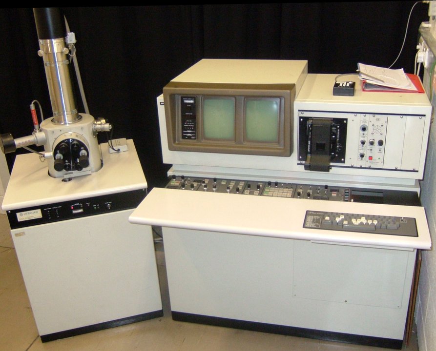
The pin identifies the verified Naka Site, established in 1961 and still responsible for semiconductor metrology, inspection equipment, and electron microscopes. The cover is a genuine Hitachi scanning electron microscope photographed at Oxford; it is not the S-6000, a CD-SEM production line, or a Japanese-site photograph, but it shows the electron-optical lineage that Naka adapted for wafer measurement.


Sources: Hitachi High-Tech electron-microscope history and Naka Area history; Hitachi High-Tech 15-year corporate history; Hitachi High-Tech Naka Site and sustainability location pages.
Photo: “Hitachi scanning electron microscope (MEB),” Steff, CC BY-SA 3.0. https://commons.wikimedia.org/wiki/File:Hitachi_scanning_electron_microscope_(MEB).jpg
changes?
delete this memory?
We detected that you have a Blox in your crypto wallet! We will import the Blox into your account.
Click on done below to complete the import.
Welcome Back!
Sign in to preserve cherished moments
Don't have an account?
Welcome!!
Sign up and start preserving cherished moments
?
?

Choose your payment method
Buy with Metablox Credit
Do you want to mint Blox with Metablox Credit?
Which Crypto would you like to use?
Purchase Confirmed!
Your Blox is being minted on-chain and will appear in your profile shortly.
Log in or sign up to claim your Blox.
How many credits do you want to buy?
$100 USD = 1 Metablox Credit = 1 Blox.
Use Metablox Credit to mint any Blox you want on the map.
expand_more








































































































