

- Home
- Semiconductor History | Japan | From Nihonbashi to Chitose
- Semiconductor History | LINTEC Itabashi — Tape Holds the Wafer While the Saw Cuts
Semiconductor History | LINTEC Itabashi — Tape Holds the Wafer While the Saw Cuts
· 1986
Personal memoryBy kevin · · updated · Report an issue

Find memories left by people near you.
Distribute Bounty
This will distribute the bounty equally among all qualifying memories. This action cannot be undone.
Cancel Bounty
Are you sure you want to cancel this bounty? The remaining amount will be refunded to your account.
Success!
Operation completed successfully.
Error
Something went wrong.
Semiconductor History | LINTEC Itabashi — Tape Holds the Wafer While the Saw Cuts
kevin

In 1986, the company then called FSK Corporation developed an industry-first UV-curable dicing tape and made a full-scale entry into semiconductor materials. The idea joined two opposite requirements in one adhesive: hold a wafer firmly while a saw divides it into individual dies, then release those fragile dies cleanly when ultraviolet light arrives.


Ordinary adhesive becomes a problem at this stage. If it grips too weakly, chips can move during cutting; if it grips too strongly, pickup can damage them or leave contamination behind. LINTEC’s tape changes adhesive strength after UV exposure. That controllable release became the basis of its Adwill semiconductor line and turned knowledge accumulated in labels, packaging tape, release papers, and precision coating into a process material hidden beneath the wafer.


The good was higher-yield handling at a critical transition between wafer fabrication and packaging. A thin consumable could reduce movement, chipping, and pickup trouble without redesigning the silicon itself. It also demonstrated a durable Japanese industrial pattern: expertise from an apparently ordinary material business could become difficult-to-replace infrastructure once it passed a chipmaker’s qualification process.
The bad sits inside that same dependence. Dicing tape is a single-use polymer product whose backing, adhesive, liner, and contaminated residue must be managed after processing. A formulation error, particle, bubble, or release problem can threaten many dies at once. Long qualifications reward reliability but make customers cautious about alternatives, while demand rises and falls with semiconductor production and packaging investment.
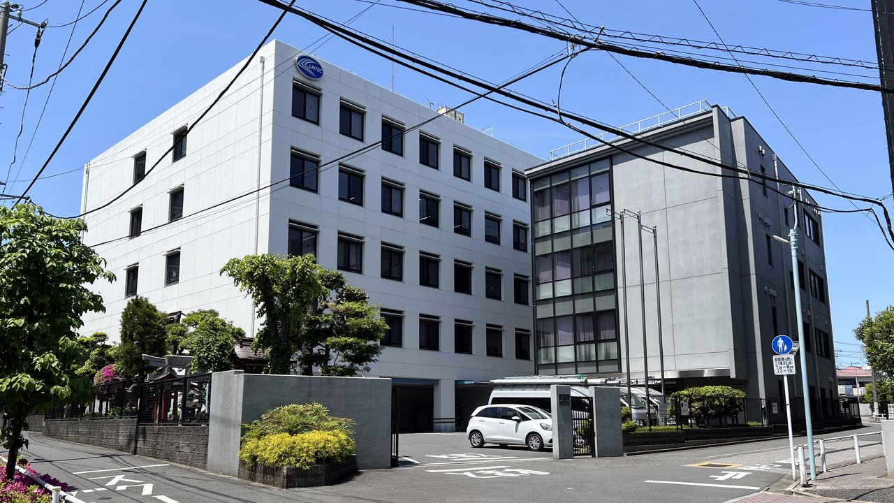
This pin marks LINTEC’s verified Itabashi headquarters, where the company had established its technical base decades before the 1986 breakthrough; it is not presented as the dicing-tape production line. The cover is a 2025 photograph of the actual headquarters, with the LINTEC name visible on the building.
Sources: LINTEC corporate history; LINTEC Integrated Reports for 2013 and 2023; LINTEC Japan location directory.
Photo: “Lintec headquarters 2025-05-03,” Asanagi, CC0. https://commons.wikimedia.org/wiki/File:Lintec_headquarters_2025-05-03.jpg
changes?
delete this memory?
We detected that you have a Blox in your crypto wallet! We will import the Blox into your account.
Click on done below to complete the import.
Welcome Back!
Sign in to preserve cherished moments
Don't have an account?
Welcome!!
Sign up and start preserving cherished moments
?
?

Choose your payment method
Buy with Metablox Credit
Do you want to mint Blox with Metablox Credit?
Which Crypto would you like to use?
Purchase Confirmed!
Your Blox is being minted on-chain and will appear in your profile shortly.
Log in or sign up to claim your Blox.
How many credits do you want to buy?
$100 USD = 1 Metablox Credit = 1 Blox.
Use Metablox Credit to mint any Blox you want on the map.
expand_more








































































































