

- Home
- Semiconductor History | Japan | From Nihonbashi to Chitose
- Semiconductor History | SUMCO Imari — Japan Consolidates for the 300-Millimeter Wafer
Semiconductor History | SUMCO Imari — Japan Consolidates for the 300-Millimeter Wafer
· 1999-7
Personal memoryBy kevin · · Report an issue

Find memories left by people near you.
Distribute Bounty
This will distribute the bounty equally among all qualifying memories. This action cannot be undone.
Cancel Bounty
Are you sure you want to cancel this bounty? The remaining amount will be refunded to your account.
Success!
Operation completed successfully.
Error
Something went wrong.
Semiconductor History | SUMCO Imari — Japan Consolidates for the 300-Millimeter Wafer
kevin

On July 30, 1999, Sumitomo Metal Industries, Mitsubishi Materials, and Mitsubishi Materials Silicon established Silicon United Manufacturing Corporation to develop and manufacture 300-millimeter silicon wafers. In 2002 it absorbed Sumitomo’s Sitix silicon business and merged with Mitsubishi Materials Silicon, then adopted the name SUMCO in 2005.

The wager was diameter. A 300-millimeter wafer holds far more dies than a 200-millimeter wafer, so a fab can spread many process steps across more saleable chips, but growing a nearly defect-free single crystal, slicing it, flattening it, polishing it, and controlling contamination become harder as the disk expands. The substrate disappears inside the finished device, yet its flatness, crystal defects, oxygen content, and surface particles set limits before a circuit pattern is printed.

The good was consolidation at the moment scale mattered. SUMCO pooled long Japanese lineages from Sumitomo, Mitsubishi, and later Komatsu, concentrated expensive crystal and polishing knowledge, and built a supplier able to qualify wafers with leading chipmakers; the Imari area became the group’s largest manufacturing site and a visible anchor for that specialization.
The bad is extreme fixed-cost and cycle exposure. Crystal pullers, polishing lines, clean utilities, and metrology must be installed before demand is certain, while customers may correct inventories for quarters; energy, ultrapure water, slurry, and discarded edge material also make every larger wafer a resource-management problem, and a defect in the substrate can waste much more value downstream.


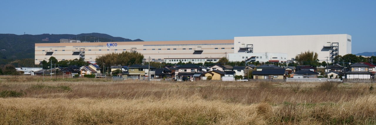
The pin uses the geotagged viewpoint of SUMCO’s Nagahama factory, whose verified business scope is the design, development, and manufacture of semiconductor silicon wafers. The photograph shows the real Imari facility in 2018, not the 1999 incorporation ceremony or a cleanroom interior.
Sources: SUMCO corporate history and corporate data; SUMCO Kyushu Factory site data and ISO 9001 scope; SUMCO securities reporting on wafer-market conditions.
Photo: “SUMCO Kyushu Imari Factory in Nagahama,” Peka, CC BY-SA 4.0. https://commons.wikimedia.org/wiki/File:SUMCO_Kyushu_Imari_Factory_in_Nagahama.jpg
changes?
delete this memory?
We detected that you have a Blox in your crypto wallet! We will import the Blox into your account.
Click on done below to complete the import.
Welcome Back!
Sign in to preserve cherished moments
Don't have an account?
Welcome!!
Sign up and start preserving cherished moments
?
?

Choose your payment method
Buy with Metablox Credit
Do you want to mint Blox with Metablox Credit?
Which Crypto would you like to use?
Purchase Confirmed!
Your Blox is being minted on-chain and will appear in your profile shortly.
Log in or sign up to claim your Blox.
How many credits do you want to buy?
$100 USD = 1 Metablox Credit = 1 Blox.
Use Metablox Credit to mint any Blox you want on the map.
expand_more








































































































