Semiconductor History | Daikin Umeda — Fluorine Etches the Pattern
volume_up
Listen
directions
Directions
In 1980, Daikin developed PFC-14, a dry-etching agent for semiconductors. Four years later it added Buffered Hydrogen Fluoride-U for wet etching, turning a fluorochemical business built alongside refrigeration into a supplier for the controlled removal of material from silicon wafers.
Etching gives a patterned resist layer physical meaning. Plasma-generated fluorine species react with selected films in a dry process, while carefully formulated hydrofluoric-acid mixtures remove silicon dioxide in wet processing; purity and reaction control determine whether the intended feature survives.
The good side was chemical leverage. Daikin already knew fluorine synthesis, purification, corrosion-resistant polymers, seals, tubes, and valves, so it could serve both the process chemistry and the equipment that safely carries aggressive materials through a fab.
Dry etching became essential as circuits moved toward smaller, more vertical structures. It can remove material directionally, helping preserve fine dimensions and form trenches or contact holes that a broadly isotropic liquid attack could not reproduce.
The semiconductor business also diversified Daikin beyond air conditioning. Its chronology shows how a corporate capability can travel: knowledge created for refrigerants and fluoropolymers became useful in gas delivery, chamber components, cleaning, and wafer-pattern transfer.
The bad side is environmental. Some perfluorocarbons used in semiconductor processing are exceptionally persistent greenhouse gases, and unreacted material or chamber-cleaning emissions must be reduced through process optimization, capture, substitution, or abatement rather than treated as invisible exhaust.
Fluorine chemistry also carries acute operational hazards. High-purity does not mean harmless: leaks, incompatible materials, moisture, and contaminated delivery systems can injure workers, damage equipment, or compromise a large volume of product.
Those risks make cylinder handling, gas monitoring, exhaust treatment, and maintenance discipline part of semiconductor yield, not merely plant utilities.
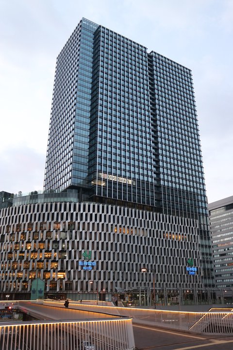
The photograph shows Daikin’s current headquarters, which the company occupied in 2022. The 1980 development predates both this building and the move; the pin is a transparent present-day corporate anchor, not the claimed laboratory of PFC-14.
Sources: [Daikin corporate chronology](https://www.daikin.com/corporate/overview/summary/history/chronology); [Daikin company history on fluorochemicals and semiconductor etching](https://www.daikin.com/-/media/Project/Daikin/daikin_com/corporate/overview/summary/history/company_history/pdf/hiraku_dl-pdf.pdf); [1999 technical review of semiconductor wet-process chemicals](https://doi.org/10.4139/sfj.50.867); [current Daikin semiconductor-materials portfolio](https://www.daikinchemicals.com/jp/solutions/industries/semiconductor-manufacturing/).
Photo: Yama0904, CC BY-SA 4.0, via Wikimedia Commons.
## Gate Summary



















































































































 expand_more