

- Home
- Semiconductor History | Japan | From Nihonbashi to Chitose
- Semiconductor History | Lasertec Shin-Yokohama — A Company Built Around Invisible Defects
Semiconductor History | Lasertec Shin-Yokohama — A Company Built Around Invisible Defects
· 1976-10
Personal memoryBy kevin · · updated · Report an issue

Find memories left by people near you.
Distribute Bounty
This will distribute the bounty equally among all qualifying memories. This action cannot be undone.
Cancel Bounty
Are you sure you want to cancel this bounty? The remaining amount will be refunded to your account.
Success!
Operation completed successfully.
Error
Something went wrong.
Semiconductor History | Lasertec Shin-Yokohama — A Company Built Around Invisible Defects
kevin

In October 1976, Lasertec, then called Nippon Jido Seigyo, developed an automated LSI photomask inspector. The machine compared repeated patterns and displayed suspected defects for an operator, replacing part of a slow visual-inspection job with a repeatable optical process.
The company had entered the chip industry a year earlier with a system for finding pinholes in photomasks. Its present Shin-Yokohama headquarters and research center came decades later, giving a growing equipment maker room to develop and assemble larger systems.

The good was turning an awkward quality-control task into a repeatable machine process. A photomask carries the pattern projected onto many dies, so one unnoticed defect can be reproduced across wafer after wafer; faster, more sensitive inspection can save far more value than the inspection tool itself costs.

Lasertec kept applying optics and measurement to increasingly difficult masks, eventually including phase-shift and extreme-ultraviolet mask systems. Its path illustrates how a relatively small specialist can become indispensable by solving a narrow problem that broad equipment companies or chipmakers do not solve as well.
The bad is the mirror image of that focus. Extreme specialization concentrates technical risk, makes revenue dependent on a small number of expensive customer programs, and gives the wider supply chain another point where a delayed tool or missed defect can constrain production.


Inspection is also economically uncomfortable: it adds no transistor and repairs no flawed design. Customers pay because the alternative — allowing an invisible error to multiply — is worse, which means the business must continually prove that higher sensitivity justifies greater tool cost and process time.
That economic logic still governs the field today.
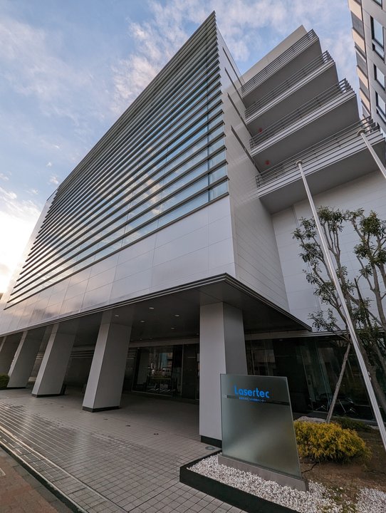
The photograph and pin show Lasertec’s actual Shin-Yokohama headquarters and R&D center from the public sidewalk. The 1976 inspector was developed decades before this facility opened, so the site represents the company’s institutional continuity, not the original workshop.
Photo: Syced, CC0, via Wikimedia Commons.
changes?
delete this memory?
We detected that you have a Blox in your crypto wallet! We will import the Blox into your account.
Click on done below to complete the import.
Welcome Back!
Sign in to preserve cherished moments
Don't have an account?
Welcome!!
Sign up and start preserving cherished moments
?
?

Choose your payment method
Buy with Metablox Credit
Do you want to mint Blox with Metablox Credit?
Which Crypto would you like to use?
Purchase Confirmed!
Your Blox is being minted on-chain and will appear in your profile shortly.
Log in or sign up to claim your Blox.
How many credits do you want to buy?
$100 USD = 1 Metablox Credit = 1 Blox.
Use Metablox Credit to mint any Blox you want on the map.
expand_more








































































































