Semiconductor History | Ricoh Ikeda — 5A22 Keeps the Super Famicom Familiar but Slow
volume_up
Listen
directions
Directions
On 21 November 1990, Nintendo released the Super Famicom in Japan. At its centre sat the S-CPU, Ricoh’s custom 5A22 processor—an evolutionary choice that helped Nintendo move beyond the Famicom without abandoning the programming lineage that had made its first console practical.
The 5A22 was built around Western Design Center’s 65C816 architecture. It could perform eight- or sixteen-bit operations and address 16 megabytes through a 24-bit address space, while retaining an eight-bit external data path.
That combination gave developers familiar 6502-family ideas in a roomier machine, though it did not make Super Famicom software directly compatible with Famicom programs.
The good part was everything Ricoh and Nintendo put around the core. The 5A22 integrated direct-memory-access controls, horizontal-blank DMA, multiplication and division hardware, interrupt timing, and controller interfaces.
DMA could move blocks while pausing the CPU; HDMA could change selected graphics registers across scanlines. Those features let a modest processor coordinate elaborate backgrounds, colour effects, and sprites with less repetitive software work.
It also extended a valuable industrial relationship. Ricoh’s Famicom chips had already turned a large Nintendo order into a bridge toward merchant semiconductors.
The Super Famicom kept that custom-silicon partnership alive: Nintendo obtained a processor shaped around its console, while Ricoh supplied another high-volume consumer LSI rather than competing only with general-purpose CPUs.
The bad part was speed. The NTSC console’s master clock was about 21.477 MHz, but the 5A22 did not execute at one simple headline rate.
Internal cycles took six master clocks, while different memory regions imposed six-, eight-, or twelve-clock accesses—roughly 3.58, 2.68, or 1.79 MHz. Performance therefore depended on where code and data lived, and the eight-bit bus serialized transfers that a wider design might have completed sooner.
That compromise aged visibly. Games could exploit DMA and the powerful picture processors, yet CPU-heavy logic and three-dimensional geometry quickly exposed the limit.
Nintendo’s later Super FX cartridges—and faster enhancement processors such as SA-1—showed both sides of the architecture: the base machine was flexible enough to accept help, but ambitious software sometimes had to bring new silicon with it.
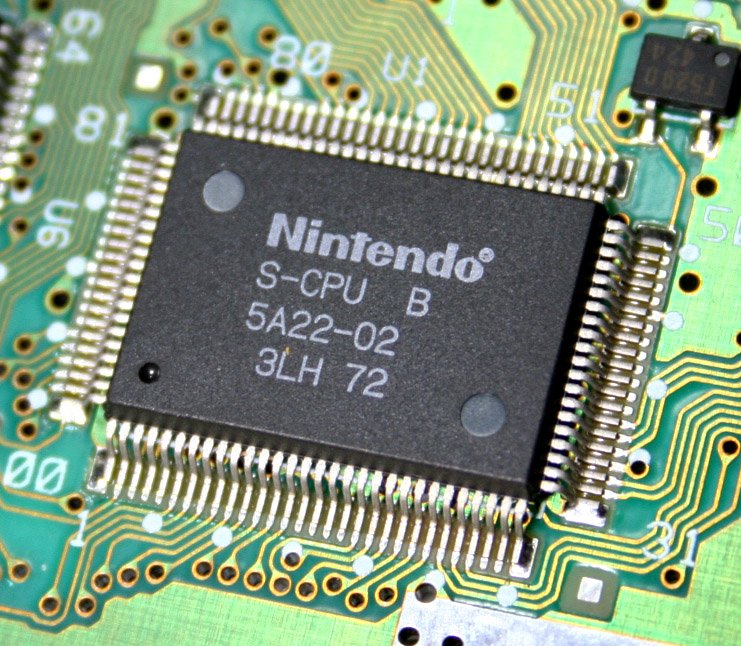
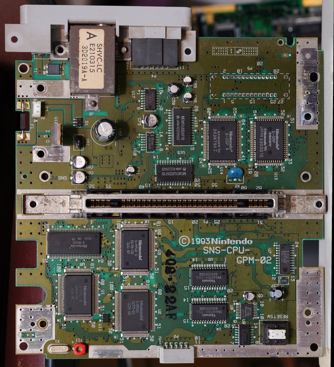
The cover photograph shows a later “S-CPU B” 5A22-02 package, not the original 1990 launch revision. The second image shows the chip among the PPU, sound, and memory devices on a later SNS-CPU-GPM-02 motherboard, providing system context rather than a launch-day board.
The pin marks today’s Nisshinbo Micro Devices Ikeda Office, successor to Ricoh’s semiconductor operations. It is an institutional lineage marker, not a claim that this exact building or room designed the 5A22.
Sources:
Nintendo, “Iwata Asks: Star Fox 64 3D”: https://www.nintendo.com/en-za/Iwata-Asks/Iwata-Asks-Star-Fox-64/Vol-1-Star-Fox-64-3D/2-It-ll-Be-Easy-to-Make-/2-It-ll-Be-Easy-to-Make--220848.html
Western Design Center, W65C816S datasheet: https://www.westerndesigncenter.com/wdc/documentation/w65c816s.pdf
Nintendo, Super Nintendo Entertainment System Development Manual, Book I: https://floating.muncher.se/bot/manual/book1_text.pdf
Anomie, “SNES timing.txt”: https://github.com/gilligan/snesdev/blob/master/docs/timing.txt
SNESdev Wiki, “Multiplication”: https://snes.nesdev.org/wiki/Multiplication
Photos:
Yaca2671, “5A22-02 01.jpg,” CC BY-SA 3.0: https://commons.wikimedia.org/wiki/File:5A22-02_01.jpg
htomari, “Nintendo SNS-CPU-GPM-02 motherboard.jpg,” CC BY-SA 2.0: https://commons.wikimedia.org/wiki/File:Nintendo_SNS-CPU-GPM-02_motherboard.jpg



















































































































 expand_more