

- Home
- Semiconductor History | Japan | From Nihonbashi to Chitose
- Semiconductor History | Sony Atsugi — The Camera Learns to See in Silicon
Semiconductor History | Sony Atsugi — The Camera Learns to See in Silicon
· 1970
Personal memoryBy kevin · · Report an issue

Find memories left by people near you.
Distribute Bounty
This will distribute the bounty equally among all qualifying memories. This action cannot be undone.
Cancel Bounty
Are you sure you want to cancel this bounty? The remaining amount will be refunded to your account.
Success!
Operation completed successfully.
Error
Something went wrong.
Semiconductor History | Sony Atsugi — The Camera Learns to See in Silicon
kevin

In spring 1970, Sony began research on charge-coupled-device image sensors. A CCD turns light into electrical charge, then shifts that charge across the chip so an image can be read out. For a company built around cameras, televisions, and recording, the device promised something radical: the camera’s “film” could become silicon.
The early results were tiny. Sony’s history records a 64-pixel image in 1972, followed by a practical sensor of roughly 120,000 pixels in 1978. Commercialization came around the turn of the decade, and in January 1980 an experimental Sony CCD camera sent images from an All Nippon Airways flight. Consumer camcorders later made the technology visible to millions.




The good was long technical persistence. Sony connected chip design, process engineering, cameras, and consumer products, giving its sensor teams a demanding internal customer as well as an external market. CCD work also created a lineage that later moved into CMOS image sensors, backside illumination, and stacked structures. Japan did not merely supply a component; it helped make digital imaging ordinary.
The bad was the cost of learning by yield loss. Dust, contamination, dark current, defective pixels, and low wafer yield could turn a promising sensor into scrap. Sony’s own history describes a serious contamination and yield crisis in 1987. Image sensors also became a concentration risk: their factories require large, repeated investment, while demand depends heavily on camera and smartphone cycles and on a relatively small number of major customers.
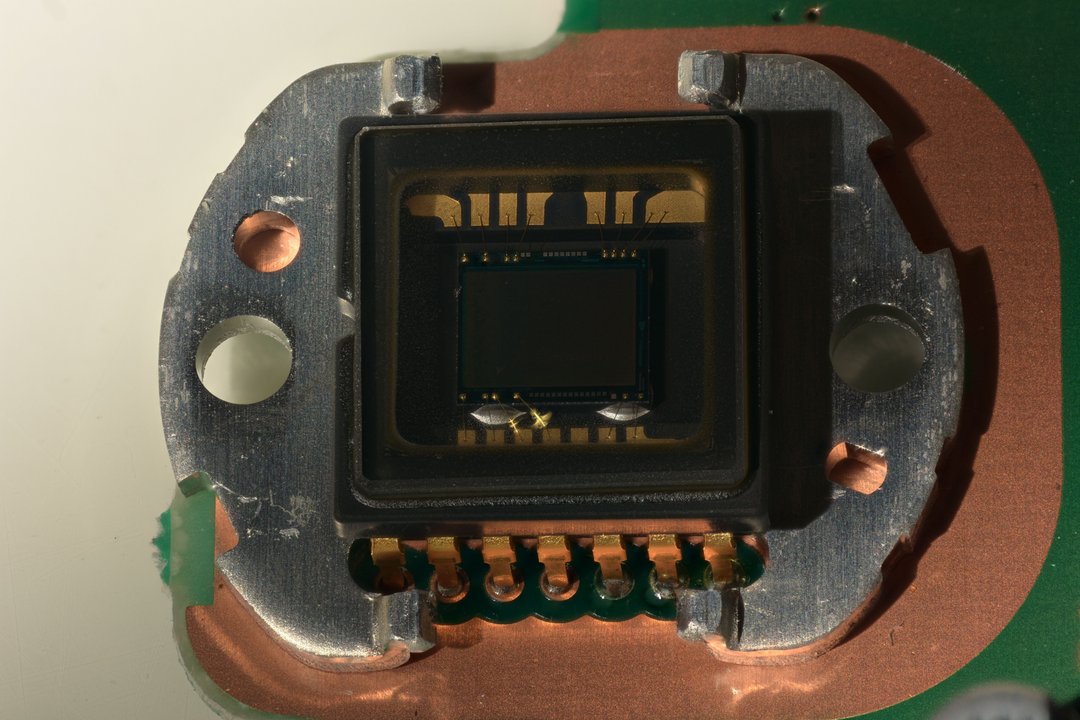
The pin marks Sony Semiconductor Solutions’ current Atsugi headquarters and design/development base, not the exact 1970 CCD laboratory; Sony says the original research began at its Central Research Institute. The cover is a focus-stacked photograph of a genuine Sony CCD-TRV24E sensor, used as a product artifact rather than a picture of the first prototype.
Sources: Sony Semiconductor Solutions, “History of Sony’s Semiconductors” and semiconductor timeline; Sony Semiconductor Solutions corporate profile and Japan operations directory.
Photo: “Sony-CCD-TRV24E sensor 88f,” Thomas Bresson / ComputerHotline, CC BY 4.0. https://commons.wikimedia.org/wiki/File:Sony-CCD-TRV24E_sensor_88f.JPG
changes?
delete this memory?
We detected that you have a Blox in your crypto wallet! We will import the Blox into your account.
Click on done below to complete the import.
Welcome Back!
Sign in to preserve cherished moments
Don't have an account?
Welcome!!
Sign up and start preserving cherished moments
?
?

Choose your payment method
Buy with Metablox Credit
Do you want to mint Blox with Metablox Credit?
Which Crypto would you like to use?
Purchase Confirmed!
Your Blox is being minted on-chain and will appear in your profile shortly.
Log in or sign up to claim your Blox.
How many credits do you want to buy?
$100 USD = 1 Metablox Credit = 1 Blox.
Use Metablox Credit to mint any Blox you want on the map.
expand_more








































































































