Semiconductor History | AGC Marunouchi — Glass Learns to Reflect EUV
volume_up
Listen
directions
Directions
In 2017, AGC began producing mask blanks for extreme-ultraviolet lithography after a development program started in 2003. The product looks like a polished plate, but it sits at one of the most demanding interfaces in leading-edge chipmaking: beneath the patterned mask that tells an EUV scanner what to print.
Ordinary transparent optics do not work at EUV’s 13.5-nanometer wavelength because the radiation is absorbed by air and most materials. The mask therefore acts as a reflector, built from a low-expansion glass substrate and many precisely controlled thin-film layers.
The good side was vertical integration. AGC could combine synthetic glass, polishing, cleaning, metrology, and coating rather than optimize one layer in isolation, giving it a way to translate a century-old glass lineage into nanometer-scale semiconductor infrastructure.
Production was the important threshold. Laboratory samples could demonstrate flatness and reflectivity, but a commercial blank also had to meet repeated customer qualifications with exceptionally low defect levels across a surface that would be copied onto many wafers.
That capability helped make EUV practical for advanced logic and memory. Shorter-wavelength patterning can replace several ArF lithography exposures in selected layers, reducing process complexity even though the EUV scanner, mask, resist, inspection, and pellicle ecosystem remains extraordinarily expensive.
The bad side is that a nearly invisible defect can become economically enormous. A particle, pit, bump, multilayer flaw, or flatness error may distort the reflected image, and defects buried below the coating can be hard to detect, classify, or repair.
The market is also narrow and capital intensive. A supplier must invest ahead of demand, protect exacting process knowledge, and serve a small number of mask shops and advanced chipmakers, while any delay in EUV adoption or shift in mask architecture can strand specialized capacity.
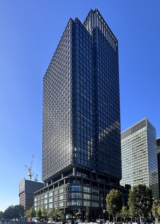
The photograph shows AGC’s current office in the Shin-Marunouchi Building, not the electronics factories that make mask blanks. The pin marks the corporate center from which the investment was governed and does not place EUV coating equipment in central Tokyo.
Sources: [AGC’s EUV development history](https://www.agc.com/en/innovation/pickup/electronics.html); [AGC production and capacity announcement](https://www.agc.com/en/news/detail/1201109_2814.html); [2007 SPIE paper on AGC mask-blank development](https://doi.org/10.1117/12.746619); [official headquarters profile](https://www.agc.com/en/company/profile/index.html).
Photo: Akonnchiroll, CC BY-SA 4.0, via Wikimedia Commons.



















































































































 expand_more