

- Home
- Semiconductor History | Japan | From Nihonbashi to Chitose
- Semiconductor History | NGK Nagoya — Ceramics Hold the Wafer Still
Semiconductor History | NGK Nagoya — Ceramics Hold the Wafer Still
· 1996
Personal memoryBy kevin · · updated · Report an issue

Find memories left by people near you.
Distribute Bounty
This will distribute the bounty equally among all qualifying memories. This action cannot be undone.
Cancel Bounty
Are you sure you want to cancel this bounty? The remaining amount will be refunded to your account.
Success!
Operation completed successfully.
Error
Something went wrong.
Semiconductor History | NGK Nagoya — Ceramics Hold the Wafer Still
kevin

In 1996, NGK—then widely known in English as NGK Insulators—began making ceramic heaters and electrostatic chucks for semiconductor production equipment. The move joined two Japanese industrial stories: a company formed around electrical porcelain in 1919, and a chip industry learning that the material touching a wafer could matter as much as the machine around it.




An electrostatic chuck holds a silicon wafer flat without ordinary mechanical clamps. A ceramic heater can warm it evenly while process gases attack, deposit, or clean surfaces only atoms thick. NGK’s strength was not chip design; it was shaping, firing, bonding, and controlling advanced ceramics so that they stayed electrically predictable, chemically resistant, and dimensionally stable inside harsh tools.
The good was enormous but mostly invisible. Better wafer holding and temperature uniformity helped manufacturers pursue tighter process windows, larger wafers, and repeatable yields. It also showed how Japan could remain indispensable even as memory-chip leadership shifted overseas: knowledge accumulated in an older industry could be redeployed into a high-value component that toolmakers and fabs had to qualify carefully.
The bad came from the same specialization. A ceramic component can be brittle, difficult to repair, and costly to manufacture when defects appear late in firing or bonding. Demand also follows semiconductor capital spending, so a supplier can face sharp cycles even when its technology remains excellent. Long customer qualifications protect incumbents, but they can also slow the adoption of a new design and concentrate revenue among a small number of equipment programs.
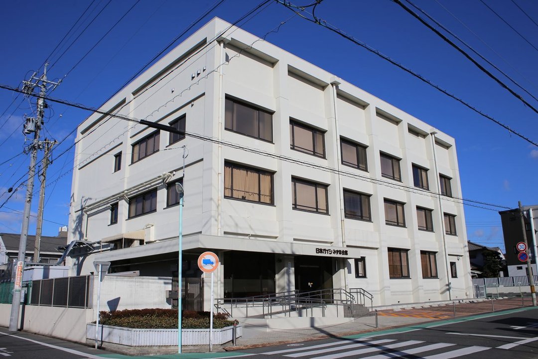
This Nagoya pin marks the corporate and engineering lineage behind the 1996 transition, not a publicly accessible cleanroom. The cover shows NGK’s nearby Mizuho Hall, photographed in 2017; it is a real company facility in the same district, not the semiconductor production line itself.
Sources: NGK corporate history and network pages; NGK annual-report material on semiconductor-production ceramics; Wikimedia Commons file page.
Photo: “Nihon Gaishi Mizuho Hall 20171217,” 円周率3パーセント, CC BY-SA 4.0. https://commons.wikimedia.org/wiki/File:Nihon_Gaishi_Mizuho_Hall_20171217.jpg
changes?
delete this memory?
We detected that you have a Blox in your crypto wallet! We will import the Blox into your account.
Click on done below to complete the import.
Welcome Back!
Sign in to preserve cherished moments
Don't have an account?
Welcome!!
Sign up and start preserving cherished moments
?
?

Choose your payment method
Buy with Metablox Credit
Do you want to mint Blox with Metablox Credit?
Which Crypto would you like to use?
Purchase Confirmed!
Your Blox is being minted on-chain and will appear in your profile shortly.
Log in or sign up to claim your Blox.
How many credits do you want to buy?
$100 USD = 1 Metablox Credit = 1 Blox.
Use Metablox Credit to mint any Blox you want on the map.
expand_more








































































































