Semiconductor History | Nintendo Kamitoba — CPU AGB Brings 32-Bit ARM to the Game Boy
volume_up
Listen
directions
Directions
On 21 March 2001, Nintendo released the Game Boy Advance in Japan around a square package marked CPU AGB. The chip moved Nintendo’s handheld line from an eight-bit SM83-compatible core to a 16.78-megahertz ARM7TDMI while retaining hardware support for older Game Boy cartridges.
The good was flexibility inside one processor architecture. ARM7TDMI could execute full 32-bit ARM instructions or the denser 16-bit Thumb instruction set, letting programmers trade richer operations for smaller code.
Nintendo’s programming manual made that choice physical. CPU AGB contained 32 KiB of fast internal work RAM on a 32-bit bus, while the separate 256 KiB work RAM used a 16-bit bus with two wait states; the cartridge interface was also 16-bit.
The manual therefore recommended 16-bit instructions for programs running from the Game Pak and 32-bit instructions for routines copied into internal RAM. Performance depended not only on what a program calculated, but on which memory held each instruction.
CPU AGB also gathered the display engine, 96 KiB of video RAM, DMA, timers, serial communication, interrupt control, and sound functions around the processor. Six graphics modes ranged from layered tile maps to direct-colour bitmap framebuffers, giving developers more freedom than the original Game Boy’s four-shade display.
Audio carried the same mixture of inheritance and expansion. Four Game Boy-compatible sound channels remained, while two Direct Sound FIFOs could accept PCM data through DMA and timers, allowing sampled speech and music without requiring a separate sound processor.
Backward compatibility extended the platform’s useful life. A physical cartridge detector selected the older hardware mode for Game Boy and Game Boy Color software, preserving an existing library instead of asking the ARM core to emulate it.
The bad was asymmetry. Only 32 KiB enjoyed the fastest 32-bit path, so larger programs constantly balanced scarce internal RAM against slower external memory and cartridge access.
Thumb code reduced storage and fetch traffic, but its compact instruction set exposed fewer registers and operations than ARM mode. Full ARM code could do more per instruction yet consumed twice as many cartridge bytes, making the best choice depend on where the routine ran.
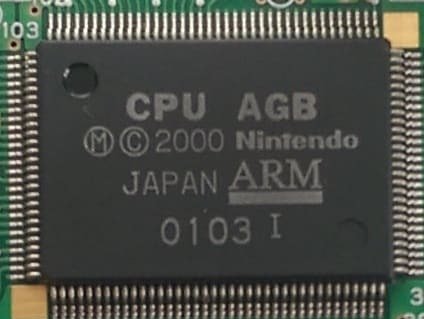
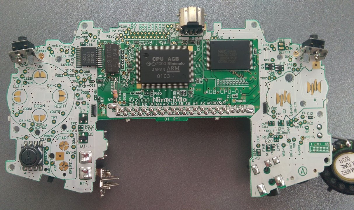
The cover is a close-up of the exact CPU AGB package marked ©2000 Nintendo, JAPAN, ARM, and 0103 I. The second photograph shows that chip on a Japanese AGB-CPU-01 motherboard assembled in early 2001, before the retail launch; neither image is an engineering prototype or a photograph of the launch event.
The pin marks Nintendo’s headquarters at 11-1 Hokotate-cho, Kamitoba, Kyoto, which Nintendo occupied after its 2000 move. It is the corporate and platform-development anchor, not a claim that this building housed the chip’s exact design room or fabrication line.
Sources:
Nintendo, Game Boy Advance hardware archive: https://www.nintendo.co.jp/n08/hardware/gba/index.html
Nintendo, Game Boy Advance Programming Manual: https://mutantstargoat.com/~nuclear/tmp/gba_prog_manual.pdf
Nintendo, corporate history: https://www.nintendo.co.jp/corporate/en/history/index.html
Nintendo, principal offices and facilities: https://www.nintendo.co.jp/corporate/en/offices/map_kyoto.html
GBATEK, GBA technical reference: https://rust-console.github.io/gbatek-gbaonly/
GBADev, CPU and memory documentation: https://gbadev.net/gbadoc/
Photos:
Gekkio (Joonas Javanainen), “Game Boy Advance CPU.jpg,” CC BY 4.0: https://commons.wikimedia.org/wiki/File:Game_Boy_Advance_CPU.jpg
Gekkio (Joonas Javanainen), “Game Boy Advance motherboard front.jpg,” CC BY 4.0: https://commons.wikimedia.org/wiki/File:Game_Boy_Advance_motherboard_front.jpg



















































































































 expand_more