

- Home
- Semiconductor History | Japan | From Nihonbashi to Chitose
- Semiconductor History | EBARA Haneda — The Pump Maker Learns to Flatten Silicon
Semiconductor History | EBARA Haneda — The Pump Maker Learns to Flatten Silicon
· 1992
Personal memoryBy kevin · · Report an issue

Find memories left by people near you.
Distribute Bounty
This will distribute the bounty equally among all qualifying memories. This action cannot be undone.
Cancel Bounty
Are you sure you want to cancel this bounty? The remaining amount will be refunded to your account.
Success!
Operation completed successfully.
Error
Something went wrong.
Semiconductor History | EBARA Haneda — The Pump Maker Learns to Flatten Silicon
kevin

In 1992, EBARA delivered its first chemical-mechanical polishing system for semiconductor production. The step turned knowledge from pumps, fluid machinery, vacuum systems, and industrial equipment into a tool that could make a patterned silicon wafer flat enough for additional wiring layers.
CMP presses a wafer against a polishing surface while slurry supplies both abrasive particles and chemical action. That combination sounds hostile to a cleanroom, but planarization became essential as chipmakers stacked more metal and insulating layers. Without a sufficiently flat surface, later lithography cannot keep every part of a wafer in focus.

The good result was a durable Japanese equipment specialty. EBARA developed a dry-in/dry-out architecture that polished, cleaned, and dried wafers inside one integrated system, reducing the chance that wet, contaminated surfaces entered the clean environment. By January 2022, the company said cumulative CMP shipments had reached 3,000 systems.

The bad side is the process burden. CMP consumes ultrapure water, pads, slurry, chemicals, filters, and replacement parts while producing a waste stream containing removed metals and abrasive material. Better recycling and process control can reduce the impact per wafer, but advanced chips require repeated planarization steps, so total consumption can still grow.
Equipment economics are equally unforgiving. A toolmaker must fund engineering, demonstration units, global service, and spare parts before customers commit to a fab cycle. A few large chipmakers can delay orders abruptly, while a field problem can create expensive retrofit obligations across an installed base.
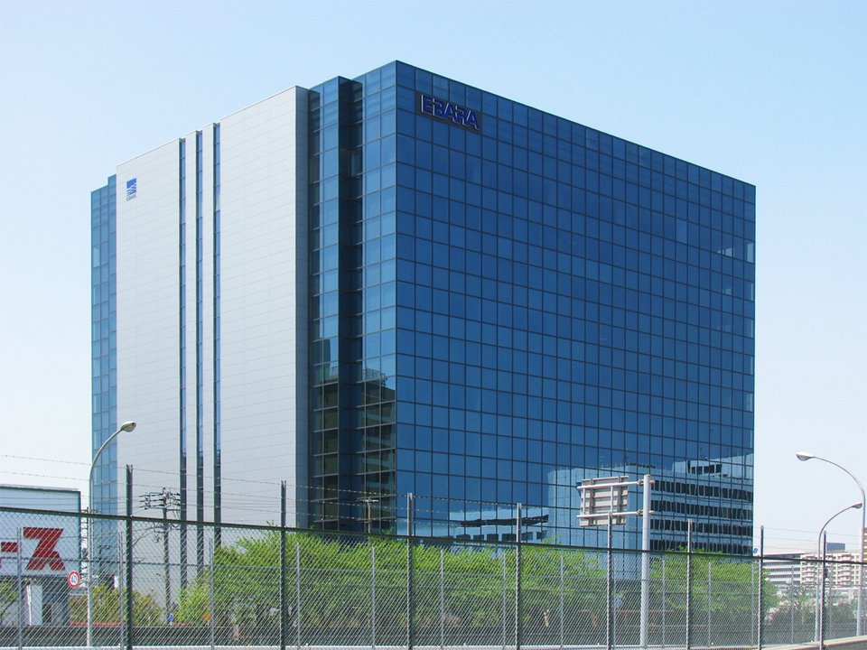
The Haneda photograph shows EBARA's present corporate headquarters, not the first 1992 CMP system or the Fujisawa operations where much precision-machinery work is performed. The exact public pin is appropriate for the company-level transition from pumps to semiconductor process equipment, with the production-site difference stated rather than concealed.


Sources: [EBARA corporate history](https://www.ebara.com/global-en/corporate/history/); [independent JBpress history of EBARA's CMP business](https://jbpress.ismedia.jp/ts/ebara_special/02/); [EBARA explanation of polishing technology](https://ebara.com/global-en/technology/information/polishing-technology-ex/); [EBARA 3,000-system release](https://www.ebara.com/jp-ja/newsroom/2022/1200953_1673/).
Photo: Aimaimyi, CC BY-SA 3.0, via Wikimedia Commons.
changes?
delete this memory?
We detected that you have a Blox in your crypto wallet! We will import the Blox into your account.
Click on done below to complete the import.
Welcome Back!
Sign in to preserve cherished moments
Don't have an account?
Welcome!!
Sign up and start preserving cherished moments
?
?

Choose your payment method
Buy with Metablox Credit
Do you want to mint Blox with Metablox Credit?
Which Crypto would you like to use?
Purchase Confirmed!
Your Blox is being minted on-chain and will appear in your profile shortly.
Log in or sign up to claim your Blox.
How many credits do you want to buy?
$100 USD = 1 Metablox Credit = 1 Blox.
Use Metablox Credit to mint any Blox you want on the map.
expand_more








































































































