Semiconductor History | Hamamatsu Photonics — Light Becomes a Semiconductor Business
volume_up
Listen
directions
Directions
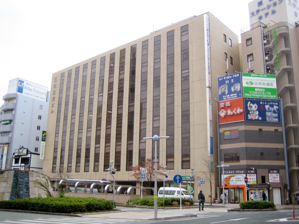
In January 1985, Hamamatsu Photonics opened its headquarters business office here in Sunayama-cho, opposite Hamamatsu Station. The office marked the scale reached by a company that had started after the war with photoelectric tubes and then learned to work on both sides of the boundary between vacuum devices and solid-state semiconductors.
The unusual part of Hamamatsu’s semiconductor history is that it never treated the chip as the whole system. Its product line grew around the problem of turning very small amounts of light into reliable electrical information: phototubes and photomultiplier tubes when extreme sensitivity mattered, silicon photodiodes and other optosemiconductors when compactness and integration mattered, then cameras, sources, and measurement systems around them.
That specialization was a strength. While Japan’s large electronics groups fought over mass-market memories and logic, Hamamatsu built difficult niches in scientific instruments, medical imaging, industrial inspection, and particle detection. Its 1982 reorganization even formalized separate Electron Tube, Solid State, and Systems divisions rather than pretending one technology would replace all the others.
The same choice carried costs. Specialist sensors sell in smaller volumes, require long qualification cycles, and often depend on customers whose experiments or instruments take years to mature. Maintaining vacuum-tube knowledge beside semiconductor fabrication is also more complicated than running a single product architecture.
The good result was resilience: Hamamatsu could select the detector physics that fitted the signal instead of forcing every problem into silicon. The bad result was a business that could be less visible, less scalable, and harder to explain than consumer-chip manufacturing.
It also complicates the usual national scorecard. Counting memory capacity or logic process nodes misses companies whose value lies in sensing, packaging light, and making weak signals usable; Hamamatsu’s history is a reminder that a semiconductor industry is wider than its largest wafer fabs.
This 2006 photograph shows the headquarters office opened in 1985, not the separate Solid State Division factory where optosemiconductors are made. The location is therefore an institutional marker for the company’s mixed technology strategy, not a claim that every device was developed inside this building.
Sources: [Hamamatsu Photonics company history](https://www.hamamatsu.com/us/en/our-company/history.html); [Hamamatsu Photonics securities report](https://www.hamamatsu.com/content/dam/hamamatsu-photonics/sites/documents/01_HQ/ir/financial-information/securities-report/h_ir_73_yuuka_j.pdf); [global-headquarters page](https://www.hamamatsu.com/jp/en/our-company/global-organizations/japan/global-headquarters/); [Integrated Report 2023](https://www.hamamatsu.com.cn/content/dam/hamamatsu-photonics/sites/documents/01_HQ/ir/integrated-report/h_ir_Integrated_Report_2023_A4_E.pdf).
Photo: Lombroso, public domain, via Wikimedia Commons.



















































































































 expand_more