- Home
- Semiconductor History | Taiwan Advanced Node Era | Tainan
- Semiconductor History | 台積電 AP8, 南科 — The Panel Fab That Became a Packaging Plant
Semiconductor History | 台積電 AP8, 南科 — The Panel Fab That Became a Packaging Plant
· 2024-8
Personal memoryBy kevin · · updated · Report an issue
Find memories left by people near you.

Distribute Bounty
This will distribute the bounty equally among all qualifying memories. This action cannot be undone.
Cancel Bounty
Are you sure you want to cancel this bounty? The remaining amount will be refunded to your account.
Success!
Operation completed successfully.
Error
Something went wrong.
Semiconductor History | 台積電 AP8, 南科 — The Panel Fab That Became a Packaging Plant
kevin
TSMC announced on 15 August 2024 that it would pay NT$17.14 billion for a building it had not designed, on land it had not chosen, to make a product the building was never built for.
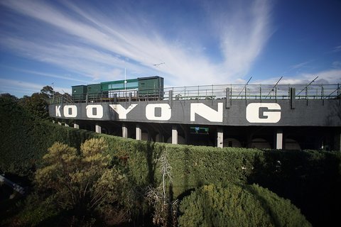
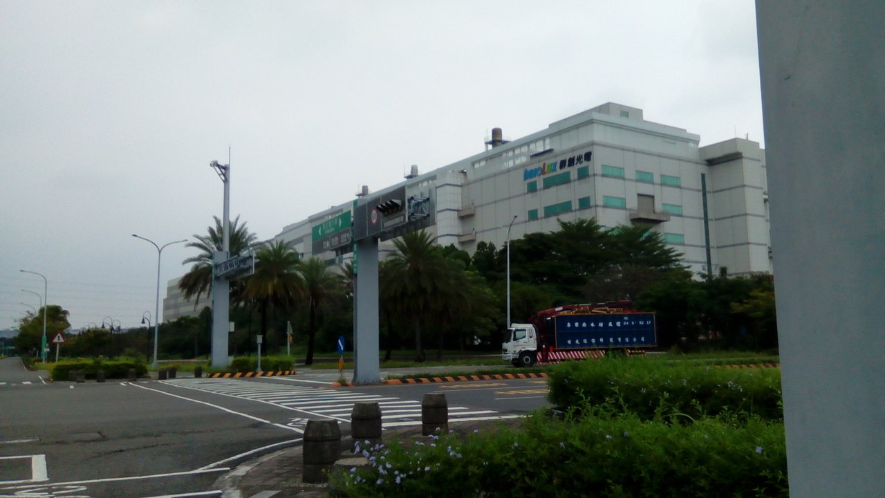
The seller was Innolux, and the property was its fourth Tainan plant, a 5.5-generation LCD panel fab.
Panels and chip packaging have almost nothing in common as processes.
What they share is a shell: a very large, very flat, structurally heavy building with a cleanroom, industrial power, ultrapure water and gas already plumbed into it, sitting on land already zoned and permitted for exactly this kind of manufacturing.
That permit was the asset.
Demand for CoWoS packaging had outrun supply, because every AI accelerator that Nvidia and its rivals sell needs logic dies and memory stacks bonded onto a silicon interposer, and the packaging step had become the bottleneck rather than the wafers.
Building a new plant in Taiwan means an environmental impact assessment measured in years.
Buying a plant that already has one means a fit-out measured in months, and that arithmetic is the whole reason this deal happened at the price and speed it did.
The site runs to about 31.7 hectares with a cleanroom close to 100,000 square metres, which makes it the largest single advanced-packaging plant TSMC operates.
Renamed AP8, the eighth in a numbered line that runs from Hsinchu through Longtan, Taichung, Zhunan and Chiayi, it took its first tools in April 2025 at a ceremony held for the supply chain, and moved toward production in the second half of that year.
Conversion has not been frictionless. Trade reporting through 2025 and 2026 describes floor-loading and utility-routing problems inherent in adapting a panel fab, and delivery slots pushed back for some equipment.
A panel plant becoming a packaging plant is also a small industrial history in itself.
Taiwan's flat-panel industry was built in the 2000s as the successor to its own earlier assembly economy, and its 5.5-generation lines were made obsolete by Chinese competition in exactly the way the industry had once made others obsolete.
The building outlived the business it was built for by finding a different one.
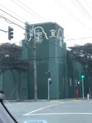
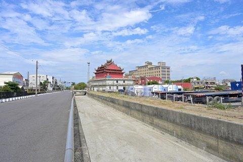
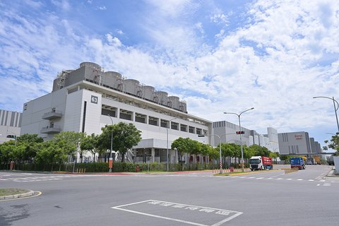
Photo: Aa7778273, CC BY-SA 4.0, via Wikimedia Commons — the Innolux plant in the Tainan park, photographed on 17 September 2019, five years before the sale and while the company's name was still on the wall.
changes?
delete this memory?
We detected that you have a Blox in your crypto wallet! We will import the Blox into your account.
Click on done below to complete the import.
Welcome Back!
Sign in to preserve cherished moments
Don't have an account?
Welcome!!
Sign up and start preserving cherished moments
?
?
Choose your payment method
Buy with Metablox Credit
Do you want to mint Blox with Metablox Credit?
Which Crypto would you like to use?
Purchase Confirmed!
Your Blox is being minted on-chain and will appear in your profile shortly.
Log in or sign up to claim your Blox.
How many credits do you want to buy?
$100 USD = 1 Metablox Credit = 1 Blox.
Use Metablox Credit to mint any Blox you want on the map.
expand_more